Fine Line Capabilities: Additive Vs. Subtractive Methods
When developing circuitry for an electronic device or product, there are two main ways to go about the process: additive and subtractive. Both processes provide advantages over the other, so neither option is better than the other for every application.
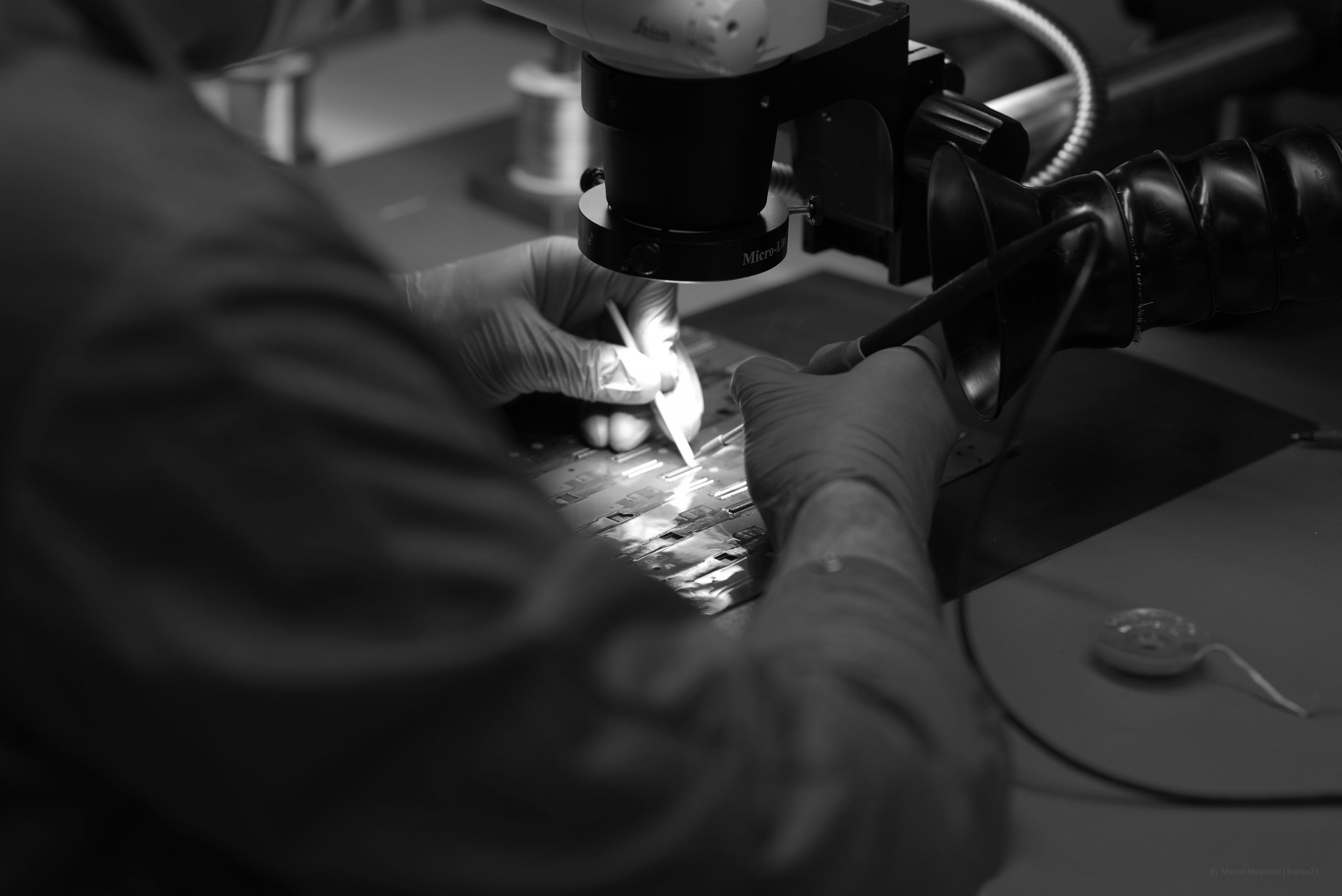
Tech Etch has the tools and technology required to provide additive or subtractive circuitry development. Our team uses state-of-the-art tools that allow us to work on circuits with conductive layers as thin as 5 microns. We have specially trained experts who know how to handle the manufacturing process to ensure the best results for any type of circuitry.
There are a few major differences between the additive and subtractive methods. Here are the basics of how these two processes differ from one another, as well as the results they produce:
The Additive Process
Using an additive process begins with a very thin layer of copper, as thin as 5 microns or less. This core material has copper on one or both sides of a polyimide film.
Resist is then coated on top of the copper surface before being imaged and developed. This process creates channels within the resist where the copper can be plated. This plated copper becomes the traces, pads, and other conductive parts of the circuit. The resist is then removed, and the background copper is etched away.
One advantage of the additive process is that it offers a resolution of .002 inch wide leads and a rectangular cross-section. Our techniques allow us to create trace and space patterns using the additive method as small as .002 inches.
The additive process allows for the development of circuits that require high density and high electrical demands.
These circuits are available with fine pitch (50-micron trace and space) and full thickness (35 microns). With this process, Tech Etch can create circuits that can handle harsh environments and keep performing. If a product requires durability, the additive process may be the right way to go.
The Subtractive Process
The subtractive process for building circuit layers works differently. It begins with copper that is bonded to one or both sides of a polyimide film. Next, resist is added to the surface, then exposed and developed. This creates openings in the resist where copper can be attacked using an etchant. After etching is complete, the resist is removed, leaving behind a perfectly etched circuit.
If you need finer pitch for your circuitry, our subtractive process can provide what you need. This process allows us to create circuits that push space and trace down to a mere 25 microns in 5-micron copper.
The additive process comes with a higher cost and more process steps compared to the subtractive process. Both additive and subtractive processes can be performed on both single and multilayer structures. This allows for even higher densities within the same footprint and for a variety of products and electronic devices.
If a product has a higher trace density, the flex can be smaller. It also leaves more room in the product packaging for additional components to be added. Higher trace density also allows for improved performance packed into the same design envelope.
When companies need circuitry developed for their products, they should talk to experts before deciding to use an additive or subtractive manufacturing process. Utilizing the right process can make a world of difference in the quality and the cost of a finished product.
Tech Etch can handle all your additive or subtractive circuitry needs. Contact us today to learn more about these processes and to get started on creating a prototype circuit for your product.