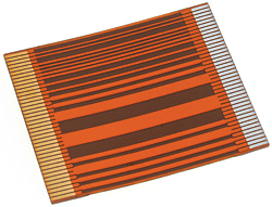
When creating circuit layers, there are two ways to go about the process. Below we break down the additive process and the subtractive process:
- Additive
Using the additive method begins with very thin (5 microns or less) copper layers on a single side or both sides of polyimide film. Resist is coated on the copper surface, imaged, and developed. This creates channels in the resist where the copper will be plated. The plated copper becomes the pads, traces, and other conductive areas of the circuit. Finally, the resist is removed and the background copper is etched away to isolate the newly created copper features.
The additive process involves more steps than the subtractive process and it costs more. On the plus side, it provides a resolution of .003 inches wide (or smaller) leads at a rectangular lead cross-section. We can create fine-line circuits using the additive process with trace and space patterns as small as .001 inches.
- Subtractive
Using the subtractive method starts with copper that is bonded to one or both sides of polyimide film. The thickness of the copper at the start of the process is the thickness it will be upon completion.
Resist is added to the copper surface, then exposed and developed. The result is openings in the resist through which the copper can be attached using an etchant. After the etching process, the resist is taken off, leaving the finished circuitry.
We can drill through flex and rigid-flex circuits to create plated through holes or mounting holes. If you need holes smaller than .008 inches, we use a laser drilling system. We can drill holes as small as .001 inches in diameter.
When drilling rigid areas, Tech Etch uses its state-of-the-art vision drilling system. This system supports registration to within .001 inches and hole diameters down to .004 inches. It can also handle blind via drilling using surface-sensing technology.
At our facility, we dedicate 30,000 square feet to finishing processes. We offer conventional and exotic surface finishes for flex circuits of all kinds.
Electroplating is the most common type of finishing we offer. This process can only be accomplished when conductors are connected to a common external bus during manufacture. When traces cannot be bussed in the panel, electroless options exist. These include hot-air solder leveling, immersion gold over electroless nickel (ENIG), and immersion tin. We can also ensure RoHS compliance if needed. Our engineers will discuss your needs to ensure you get the services you require.
Exposed pads will usually require a finish for corrosion-resistance or compatibility with the assembly process. We offer electroplating of gold, copper, lead, and tin.
| Finish | Min. Thickness (in.) | Max. Thickness (in.) | Tolerance |
|---|---|---|---|
| Hard Gold | .000010 | .000200 | Min. |
| Soft Gold | .000010 | .000200 | Min. |
| Tin | .000050 | .000200 | +/- 25% |
| Tin-lead | .000050 | .000500 | +/- 25% |
| Cu-Tin | – | – | – |
| Nickel | .000050 | .000200 | +/- 40% |
| Hot Air Level | N/A | N/A | N/A |
With the help of our in-house electroplating and precision imaging tools, we can provide circuits with selective finish plating, as well. This process allows for different plating on different areas of your circuits. This can be very useful when many assembly processes will be used.

