Materials, Layers & Vias
Copper is the most common material used for creating circuit traces. The thickness of our products ranges from .0007 inches to .0028 inches. We work with adhesive and adhesive-free substrates.
Tech-Etch uses copper for circuit traces as it offers the most cost-effective solution. However, we can also use:
- Stainless steel (for corrosion resistance)
- BeCu (for its spring properties)
- Cupronickel (for high-resistance applications)
- Tungsten (for radiopacity)
Take a look at our flex circuit construction page to learn more about our processes.
When it comes to insulation, polyimide film is the most common material used for flex circuits. We use this film as the inner layers of multilayer circuits, as well as the base layer on single-metal-layer flex circuits.
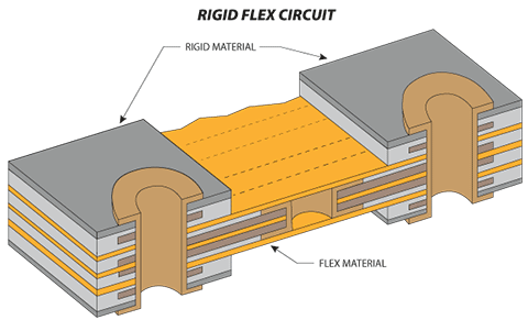
Pre-preg and FR-4 work together to create the entire insulating layers at the rigid area of a rigid-flex circuit. The team at Tech-Etch can work with common laminates and pre-pregs, including high-speed and high-Tg/Td materials.
Through-vias are metalized holes that goes through every layer of a flexible circuit, connecting two or more conductive layers. We can offer circuits with plated-through, buried, or blind vias.
Blind vias connect and outer layer with an adjacent layer of the circuit without going through the entire circuit. Buried vias create a connection between inner layers without touching the outer layers. These via types can increase space inside a circuit when you need to add features like component pads or additional trace routes.
Even rigid-flex products can benefit from the via process in certain circumstances. The process involves filling the via with conductive or non-conductive epoxy. It continues with planarizing and plating over the material, resulting in a smooth and flat via capture pad. This process also makes it suitable as a component attachment pad.
We can drill vias as small as .001 inches in diameter. Take a look at our tolerance page for more details.

